ASIC Miner ICERIVER KAS KS0 Profitability In the realm of cryptocurrency mining, the Iceriver KAS KS0 miner has garnered widespread attention. Tailored specifically for the Kaspa network's KHeavyHash algorithm, it boasts high hashing power and low power consumption, making it an ideal choice for many miners. In this article, we will comprehensively assess IceRiver KS0 profitability while considering the Kaspa market conditions and the attributes of KS0 miner. Kaspa Market Dynamics Kaspa is a vibrant cryptocurrency network aimed at delivering high performance and scalability for everyday transactions. At the time of writing this article, the Kaspa coin trades at approximately $0.04959. But it's essential to note that cryptocurrency markets are highly susceptible to price volatility. Hence, investors must remain vigilant about market dynamics. Additionally, the Kaspa network's mining difficulty and reward mechanisms play a role in mining returns. Attributes of the IceRiver KS...
What is Antminer control board CPU chip ZYNQ XC7Z010?
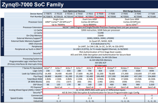
XILINX took the lead in integrating the dedicated central processing unit CPU core and FPGA into one chip, resulting in a new heterogeneous platform called All Programmable SoC; the birth of ZYNQ series chips, It has played a massive role in promoting the development of global information technology. On the one hand, the design structure of the embedded system is more flexible, the volume is significantly reduced, and the reliability and overall system performance are significantly improved; on the other hand, the FPGA can enter the application field of the embedded system, which significantly expands the application scope of FPGA.The main control chip of the ZYNQ7010 control board adopts the Xilinx ZYNQ XC7Z010 of the ZYNQ7000 series of Xilinx Company; the specific model is XC7Z010CLG400-1. ZYNQ is divided into PS and PL two parts. The PL part has 28K logic units, 2.1Mbits of embedded storage resources, 80 DSP units, 2 clock management units (CMT), 16 global clock networks, 5 users I/OBANK, and a maximum of 228 users I/O, ZYNQ XC7Z010 control board main control chip can be widely used in all Antminers, for example Antminer L7, Antminer S19 XP, Antminer T19, etc. it is a very cost-effective chip.
The main control chip of the ZYNQ7020 control board adopts the ZYNQ XC7Z020 of the ZYNQ7000 series of Xilinx Company; the specific model is XC7Z020CLG400-2. The PL part has 85K logic units, 4.9Mbits of embedded storage resources, 220 DSP units, 4 clock management units (CMT), 16 global clock networks, 6 users I/OBANK, and a maximum of 253 users I/O.
The XC7Z020 and XC7Z010 integrate two Cortex-A9 processors, AMBA® interconnect internal memory, external memory interface, and peripherals. ZYNQ-7000 integrates ARM Cortex-A9 dual-core processor (hardcore) + FPGA features of the Artix 7 series. The following are the resources included in ZYNQ-7000:
It can be seen from the above table that Zynq®-700 includes ten chips, including Xilinx ZYNQ XC7Z007S, XC7Z012S, XC7Z014S. Among them, 7010 includes Dual-Core ARM Cortex-A9 MPCore and rich peripherals, FPGA lists the number of LUTs, FF, BRAM, and DSP Slices (IP without PCIe);
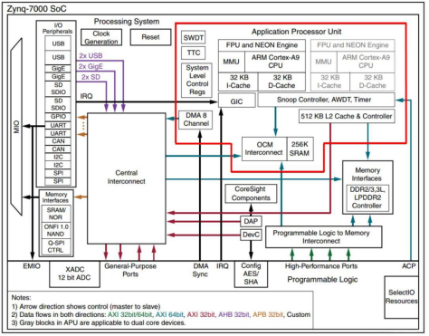
Its internal interconnection structure is as follows:
Its internal interconnection structure is as follows:
Two ARM Cortex-A9 cores with L1/L2 Cache, with MMU, FPU & NEON engine, internal on-chip memory OCM (On-Chip Memory), rich peripherals, and GIC interrupt controller; the lower part is the FPGA part, which uses the AXI bus to pass Interconnect forms an interconnection structure with CPU hardcore and external parts;
The speed grade of the XC7Z020-2CLG400I chip is -2, industrial grade, the package is BGA400, and the pin pitch is 0.8mm.
The XC7Z010-1CLG400C chip has a speed grade of -1, commercial grade, and is packaged in a BGA400. The specific chip model definition of the ZYNQ7000 series is as follows:
The speed grade of the XC7Z020-2CLG400I chip is -2, industrial grade, the package is BGA400, and the pin pitch is 0.8mm.
The XC7Z010-1CLG400C chip has a speed grade of -1, commercial grade, and is packaged in a BGA400. The specific chip model definition of the ZYNQ7000 series is as follows:
In addition, when we use the BGA packaged chip, the chip pin name changes to the form of letters + numbers, such as A1, C2, etc., so when we look at the schematic diagram, we see letters + numbers in this form, which is Represents the pins of the BGA.
The actual picture of the ZYNQ chip is shown in the middle of the figure below (take the Xilinx ZYNQ-7010 as an example).
The actual picture of the ZYNQ chip is shown in the middle of the figure below (take the Xilinx ZYNQ-7010 as an example).


Comments
Post a Comment
Tell us your opinion