ASIC Miner ICERIVER KAS KS0 Profitability In the realm of cryptocurrency mining, the Iceriver KAS KS0 miner has garnered widespread attention. Tailored specifically for the Kaspa network's KHeavyHash algorithm, it boasts high hashing power and low power consumption, making it an ideal choice for many miners. In this article, we will comprehensively assess IceRiver KS0 profitability while considering the Kaspa market conditions and the attributes of KS0 miner. Kaspa Market Dynamics Kaspa is a vibrant cryptocurrency network aimed at delivering high performance and scalability for everyday transactions. At the time of writing this article, the Kaspa coin trades at approximately $0.04959. But it's essential to note that cryptocurrency markets are highly susceptible to price volatility. Hence, investors must remain vigilant about market dynamics. Additionally, the Kaspa network's mining difficulty and reward mechanisms play a role in mining returns. Attributes of the IceRiver KS...
How many types of chips are on the Antminer S17 Pro hash board?
The chip types on the Antminer S17 Pro hash board mainly include ASIC chips, converter chips, voltage regulator chips, memory chips, temperature sensor chips, MOS chips, controller chips, and voltage monitoring chips. What role does it play in it? We together look!
Easily damaged parts of Antminer S17 Pro hash board introduction
1. BM1397AD ASIC chip
A single S17 Pro hash board has 48 BM1397AD chips located under the heat sink on the front of the hash board and connected to the heat sink through thermosetting adhesives. They are mainly responsible for the hash rate calculation of the whole miner. Therefore, if the hash rate of a single chip is low during the operation, it will result in a low hash rate and no hash rate for the entire hash board.
2. Converter chip
1) CT1F
SN74LVC1T45DBVR CT1F is a 6-pin dual power bus transceiver chip IC; using SOT-23-6 packaging technology, the operating voltage is between 1.65V~5.5V, and the operating temperature is between -40℃~+80℃.
2) U7: MPSK461517DR877500
The MPSK391517DR is a 3A, 25V, 1.1MHz boost converter chip in a tiny 4mm*4mm 16-pin QFN package. The output voltage is between 2.6V-25V, and its chips feature under-voltage lockout protection, soft-start operation, and zero-current shutdown mode.
3. Voltage regulator chip
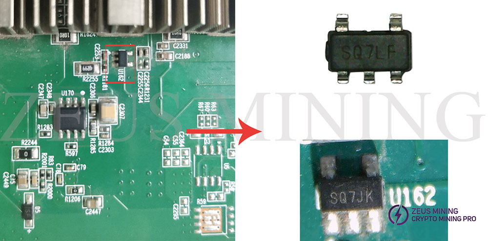
1) U162: SQ7JK SGM2036-ADJ
SGM2036-ADJ adopts SOT-23-5 package technology; its input voltage is between 1.6V and 5.5V, providing up to 300mA output current. It is a low-power, low-dropout CMOS linear regulator that is also perfect for low-voltage, low-power applications.
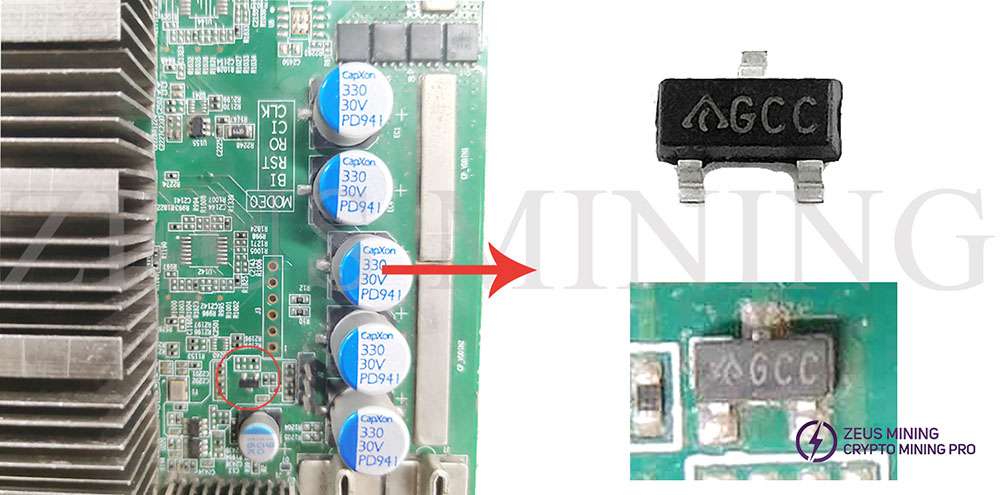
2) GCC AP431SAN1TR-G1
The AP431SAN1TR-G1 is a 3-terminal adjustable shunt regulator in SOT23 package technology. With its sharp turn-on characteristics, the AP431SAN1TR has a low minimum cathode current for regulation, with a typical value of 50µA, making the device ideal for very low power applications. Additionally, two levels of initial voltage tolerance are available at +25°C, 0.5%, and 1%.
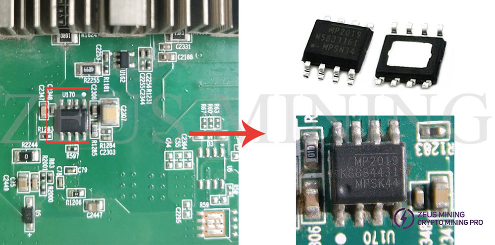
3) U170: MP2019K8884431MPSK44
MP2019K8884431MPSK44 is the product number of the MP2019 series of linear regulators, using SOIC-8 EP package technology, 3V-40V voltage input range, -40°C to +125°C junction temperature range, is a 40V 300mA, low static current adjustable output linear regulators.
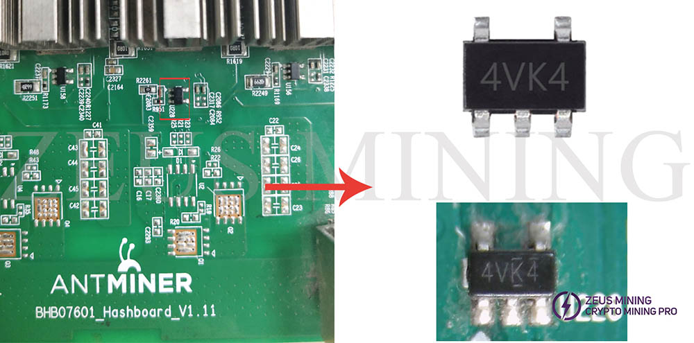
4) U228: LN1134A182MR-G 4VK4
LN1134A182MR-G 4VK4 is a high-speed, low-dropout, high-precision output voltage, low-consumption current positive voltage hash board voltage-domain regulator chip developed by CMOS technology. Its built-in low on-state resistance transistor provides over-current protection for the chip. Its output voltage is between 1.0V and 5.0V, and the maximum output current is 300mA.
4. EEPROM chip
U6: ATH93702DMCN1937
The ATH91502DMCN provides 2,048-bit-serial electrically erasable and programmable read-only memory. The chip adopts 8-pin TSSOP, a built-in bidirectional data transmission protocol compatible with 400kHz (1.7V) and 1MHz (2.5V) simultaneously, data storage time is long, and its operating voltage is between 1.7V~ 3.6V.
5. Temperature sensor chip
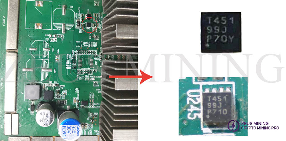
U245: T451 temperature sensor
The S17 Pro hash board has 4 built-in T451 temperature sensorchips, using WSON-8 packaging technology, mainly used to sense the temperature of the hash board. If the temperature sensor chip is damaged, it will cause abnormal temperature readings. Likewise, if the temperature sensor chip temperature is too low, the hash board will not start, or if the temperature is too high, the miner will stop running.
6. MOS chip
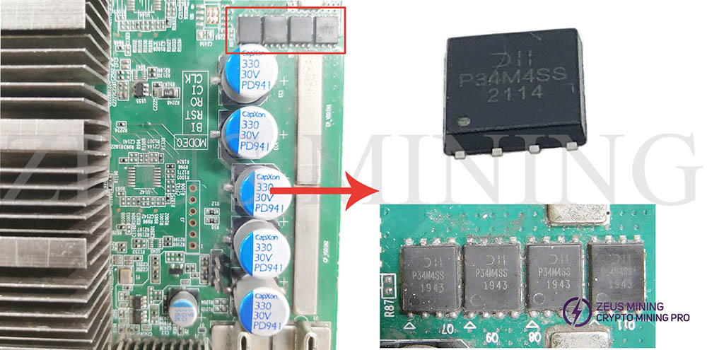
Q11: MOS DMP34M4SPS-13
MOS DMP34M4SPS-13 is a P-channel enhancement mode MOS designed to minimize RDS(ON) and maintain excellent switching performance, and this chip is mainly suitable for power management and load switching.
7. Controller chip
U3: dsPIC33EP16 GS202 PIC chip
The dsPIC33EP16 GS202 adopts SOIC-28 package technology and is a 16-bit processor and microcontroller chip.
8. Voltage monitoring chip
U252: SXE1923
The SXE1923 voltage monitoring chip is used to monitor the real-time voltage of the hash board voltage domain. If the chip is damaged, the front boost chip will not be able to receive the returned data and stop working, causing the hash board to fail to start.





Comments
Post a Comment
Tell us your opinion