ASIC Miner ICERIVER KAS KS0 Profitability In the realm of cryptocurrency mining, the Iceriver KAS KS0 miner has garnered widespread attention. Tailored specifically for the Kaspa network's KHeavyHash algorithm, it boasts high hashing power and low power consumption, making it an ideal choice for many miners. In this article, we will comprehensively assess IceRiver KS0 profitability while considering the Kaspa market conditions and the attributes of KS0 miner. Kaspa Market Dynamics Kaspa is a vibrant cryptocurrency network aimed at delivering high performance and scalability for everyday transactions. At the time of writing this article, the Kaspa coin trades at approximately $0.04959. But it's essential to note that cryptocurrency markets are highly susceptible to price volatility. Hence, investors must remain vigilant about market dynamics. Additionally, the Kaspa network's mining difficulty and reward mechanisms play a role in mining returns. Attributes of the IceRiver KS...
The important chips on the Antminer S17 + hash board
A hash board can have as few as dozens or hundreds of chips, including ASIC chips, converter chips, memory chips, temperature-sensing chips, MOS chips, etc. Where are these chips located? What role do they play on the hash board? Let's take a look!
Easily damaged parts of Antminer S17+ hash board introduction
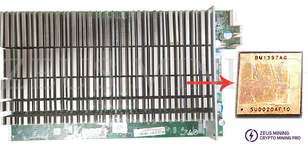
BM1397AG ASIC chip:
The ASIC chip is the most significant number of hash board chips. The entire board has a total of 65 BM1397AG ASIC chips. They are distributed under the dense heat sink and are connected to the heat sink through thermosetting adhesives. They are mainly responsible for the hash rate calculation of the whole machine. If one of the ASIC chips is damaged, the miner will have no or low hash rate.
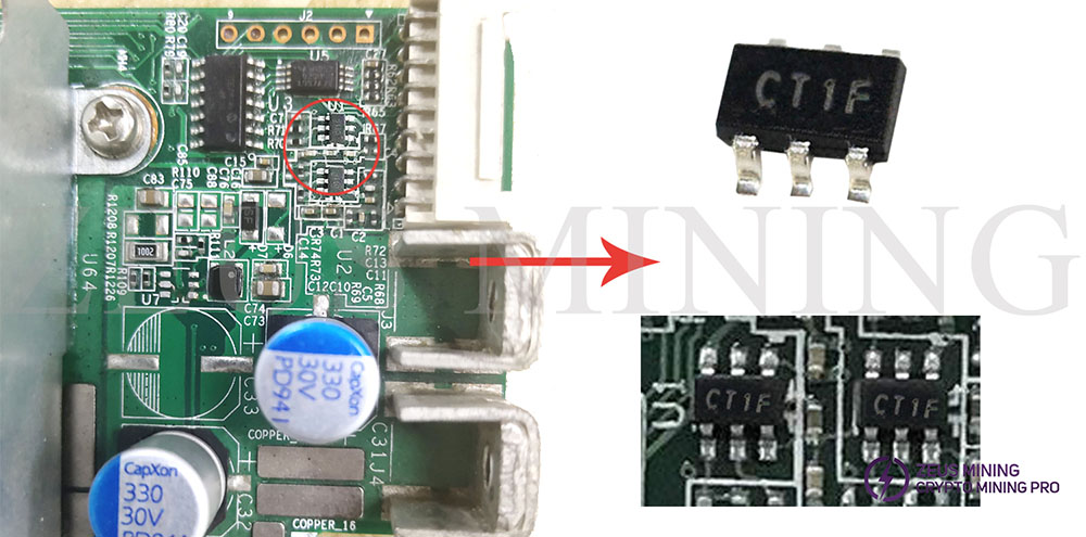
U1: CT1F
SN74LVC1T45DBVR CT1F is a 6-pin dual power bus transceiver chip IC. There are 2 CT1F chips in the entire hash board. They are located in the upper right corner of the front of the hash board. They use SOT-23-6 packaging technology, and the working voltage is between 1.65V and 5.5V, and the working temperature is between -40°C and +80°C.
U3: PIC16F1704
PIC16F1704 is an 8-bit microcontroller mainly used for checking PIC circuits. For example, when the PIC pin voltage does not reach the standard value, you can re-program the PIC by checking whether the connection between the test fixture cable and the hash board is normal.
U5: ATH93702DMCN
The ATH91502DMCN provides 2,048-bit serial electrically erasable and programmable read-only memory. In addition, the chip has a built-in two-way data transmission protocol, long data storage time, and operating voltage between 1.7V and 3.6V.
Q1: TPHR9003NL
The MOS Chip TPHR9003NL is mainly used to check the voltage output in the voltage domain. By measuring the output of the power supply terminal of the hash board, it can judge whether the MOS is short-circuited (measure the resistance between pins 1, 4, and 8). Under normal circumstances, the voltage is unstable, and the lightning surge will cause damage to the MOS.
U6: 1517DR
The MPSK391517DR chip is located in the lower right corner of the front of the Hash board and is a boost converter chip in a tiny 4mm*4mm 16-pin QFN package technology. The MP1517DR regulates the output voltage to 25V with up to 95% efficiency. In addition, its current mode regulation and external compensation components allow the MP1517DR control loop to be optimized over a wide range of input, output, and load current conditions.
U4: GCC AP431SAN1TR-G1
The AP431SAN1TR-G1 chip is located in the lower right corner of the back of the hash board and is a 3-terminal adjustable shunt regulator using SOT23 packaging technology. With its sharp turn-on characteristics, the AP431SAN1TR has a low minimum cathode current for regulation, with a typical value of 50µA, making this chip ideal for low-power applications.
U28: MP2019K3869253MPSK34
MP2019K3869253MPSK34 is the product number of the MP2019 series of linear regulators. The chip is located at the upper right of the back of the Hash board. It adopts SOIC-8 EP packaging technology and has a voltage input range of 3V-40V. It is a 40V 300mA, low quiescent current adjustable output linear regulator.
U127: SQ7JK SGM2036-ADJ
The SGM2036-ADJ chip is located above the back of the hash board; it is a low power, low dropout, CMOS linear regulator with an input voltage between 1.6V and 5.5V, providing up to 300mA of output current, perfect for low voltage, low power applications.
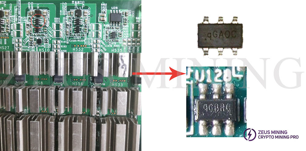
U128: qGBRC SY8120I
The qGBRC chip, located directly above the hash board, is a high-efficiency, synchronous step-down DC/DC converter capable of delivering 2A of load current. The chip integrates main and synchronous switches with very low RDS(ON) to minimize conduction losses.
U120: T2F NCT218
NCT218 temperature sensor chip is a temperature sensor chip with a dual-channel digital thermometer and under-temperature / over-temperature alarm, and it can be accurate to ±1.75°C Hash board ambient temperature. The temperature reading will be abnormal when the temperature sensor chip is damaged. When the temperature sensor chip temperature is too low, the hash board will not start. When the temperature is too high, the miner will stop running.


Comments
Post a Comment
Tell us your opinion