ASIC Miner ICERIVER KAS KS0 Profitability In the realm of cryptocurrency mining, the Iceriver KAS KS0 miner has garnered widespread attention. Tailored specifically for the Kaspa network's KHeavyHash algorithm, it boasts high hashing power and low power consumption, making it an ideal choice for many miners. In this article, we will comprehensively assess IceRiver KS0 profitability while considering the Kaspa market conditions and the attributes of KS0 miner. Kaspa Market Dynamics Kaspa is a vibrant cryptocurrency network aimed at delivering high performance and scalability for everyday transactions. At the time of writing this article, the Kaspa coin trades at approximately $0.04959. But it's essential to note that cryptocurrency markets are highly susceptible to price volatility. Hence, investors must remain vigilant about market dynamics. Additionally, the Kaspa network's mining difficulty and reward mechanisms play a role in mining returns. Attributes of the IceRiver KS...
Antminer S9 teardown report
Next, welcome to follow us to see the detailed teardown report of Antminer S9, which includes: the complete teardown high-definition picture, BOM table of each board, teardown analysis report, mining income calculation, etc.
I. the complete teardown HD full picture
Antminer S9 main components: control board + hash board + power supply
▼
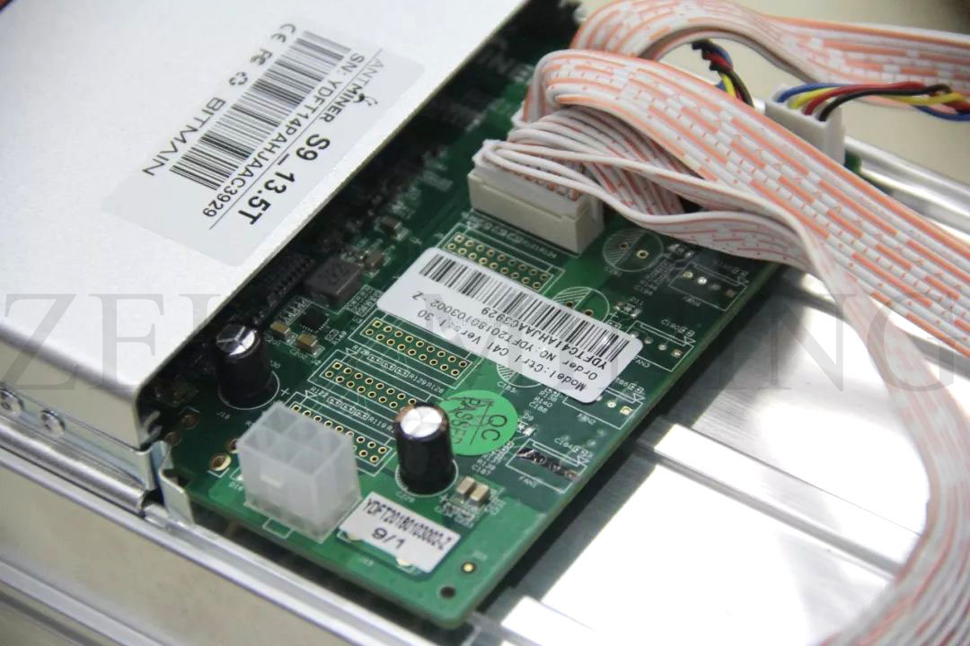
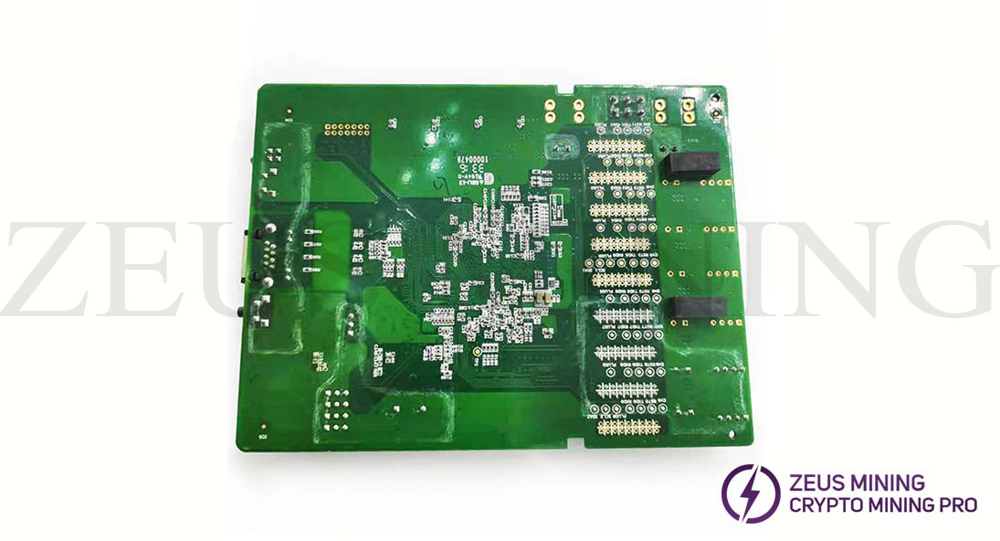
Antminer S9 control board teardown
▼
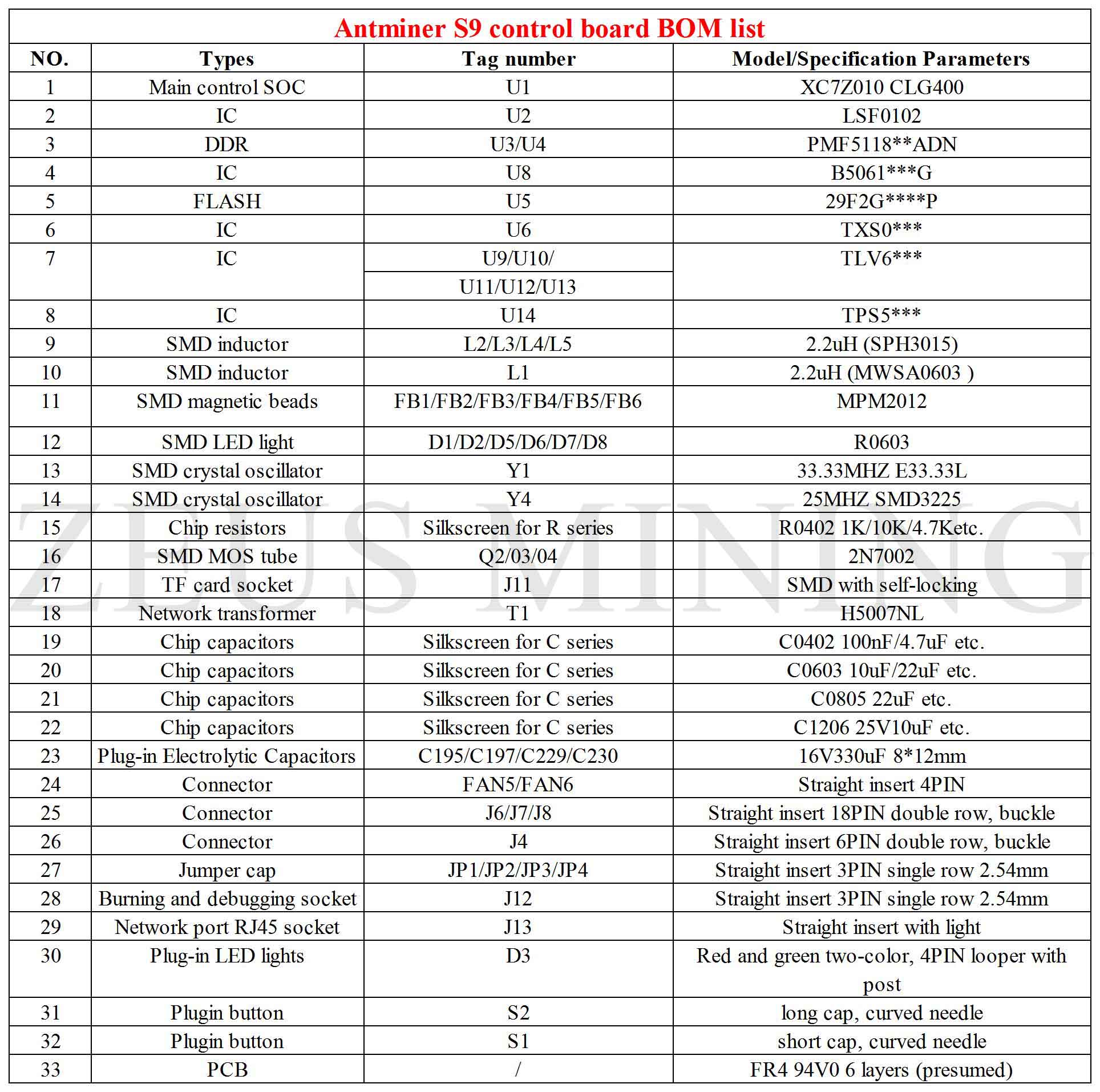
Antminer S9 control board BOM list
▼
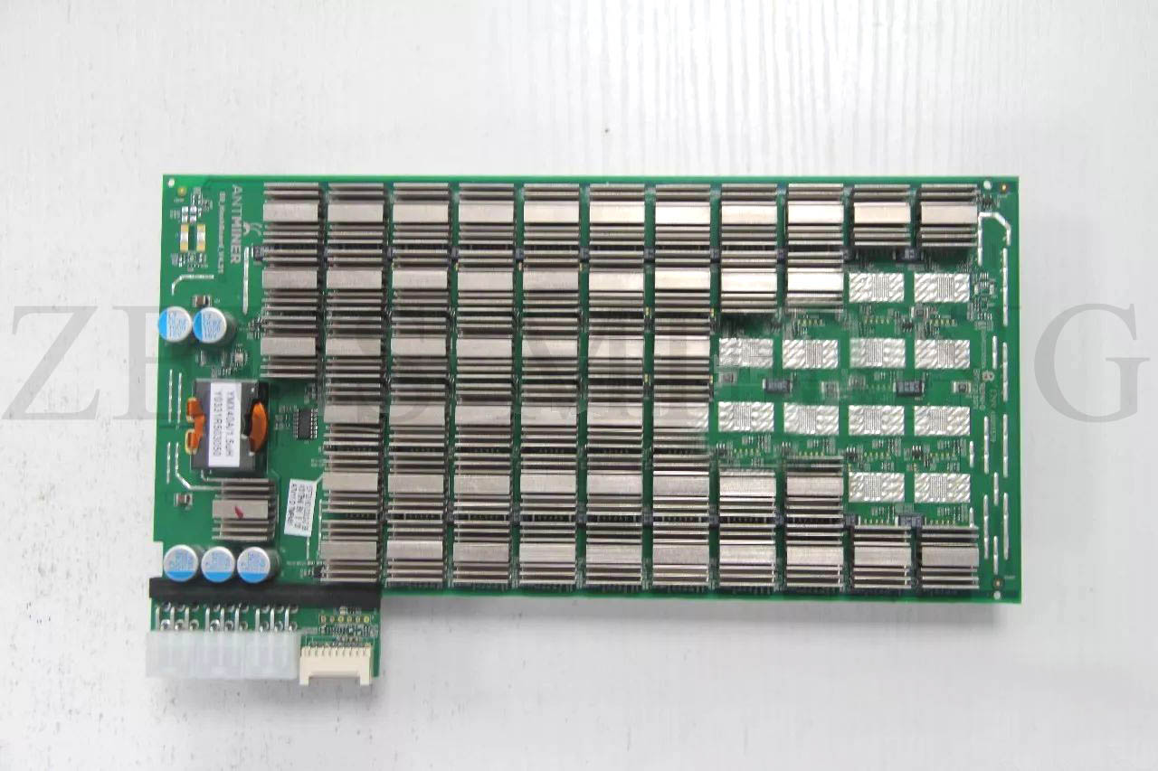
Antminer S9 hash board
▼
Below the 3 blue and white data cables are the 3 hash boards of the Antminer S9.
Antminer S9 hash board front
▼
Below the dense heat sink are the miners' ASIC chips, and each hash board carries 63 ASIC chips.
Antminer S9 hash board back
▼
The fins on the back and the front are different in height and material and are specially treated.
Hash board and ASIC chip after removing the heat sink
▼
After removing all the heat sinks, the 63 BM1387 ASIC chips were fully revealed.
Enlarged renderings
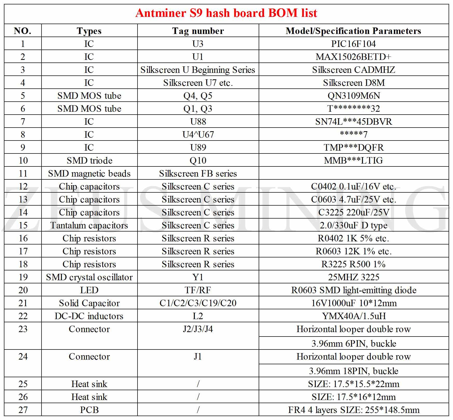
Antminer S9 hash board BOM list
▼
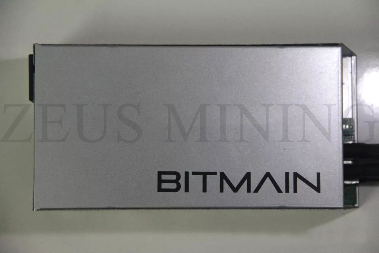
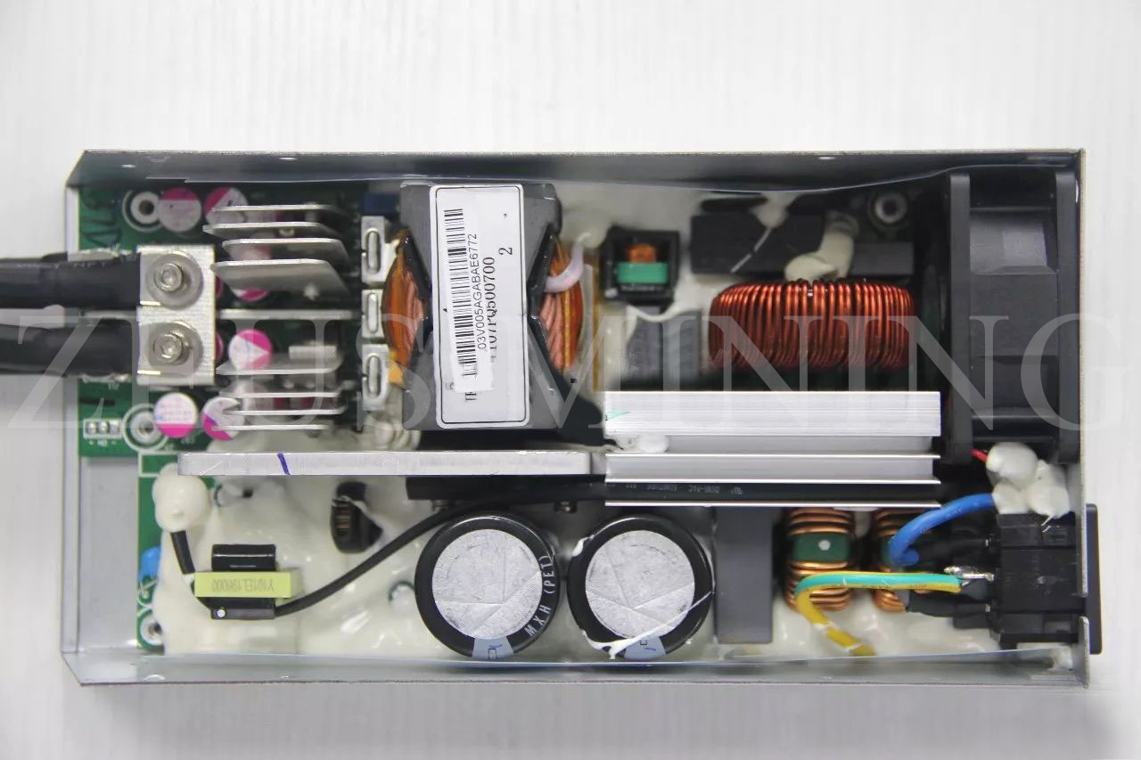
Official Power Supply for Bitmain S9
▼
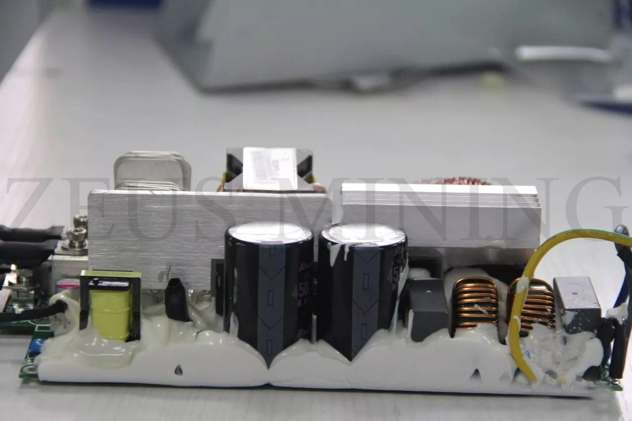
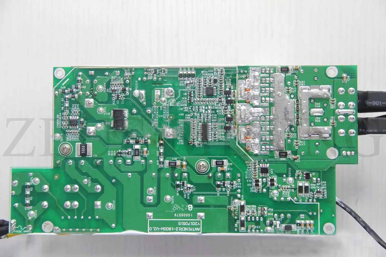
Official power supply teardown of Bitmain S9
▼
Antminer S9 power supply board BOM list
▼
II. Teardown analysis report
The S9 miner control board adopts Xilinx's latest Zynq-7000 All Programmable SoC platform based on the 28nm process flow. It selects Zynq-7010 as the processor to tightly integrate the ARM processor and FPGA architecture. The unit has a dual-core ARM Cortex-A9 MPCore (667M ), high performance and low power consumption, and meets the miner's needs. The following is the functional structure diagram of the miner control board:
The picture above shows that the main control board is equipped with a serial port, network port, TF card, and other interfaces and supports output expansion (9 hash boards can be connected).
Design advantages:
From the BOM list and the actual PCBA, we can see that the control loop is designed with detailed consideration:
1. The function expansion of the product is better considered in the circuit design process of the control board. This control board can support driving 9 pieces of hash boards.
2. Hash board chips all use an independent power supply, and each chip uses discrete heat sinks for heat dissipation.
3. When designing, it is more common to use materials for packaging, and there are no special-shaped parts. The material brand quality is stable, and the control board power supply DC-DC chip adopts a TI chip. TI's industrial-grade product TPS51200 is used in the DDR Power circuit design to match VTT, guaranteeing signal quality.
4. The connectors of the core board are all sockets with locks, which can prevent the loose cables of miners during transportation or use.
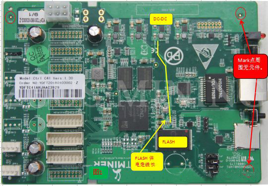
5. When the PCB LAYOUT of the whole miner is used, the design rules are better followed: it is forbidden to place components within 5mm of the Mark point (refer to the red symbol in the physical picture 1 below); the placement of SMT components is relatively regular, without particular angles, SMT manufacturing efficiency High; ETH/DDR and other circuits are designed with impedance matching to ensure the integrity of the signal. The Power/GND network reference layer is relatively complete; the functional chip layout is reasonable, the PCB shape is square, and the high utilization rate.
Inadequate design:
1. The safe distance is not guaranteed during the PCB LAYOUT of some circuits of the power board.
2. The average distance between the TF cardholder and the S2 button is not maintained, which is not conducive to the manufacture and after-sales maintenance of the DIP plug-in.
3. The NAND FLASH body of the control board and its power supply chip are far away and pass through the middle of the ETH and SOC. From the perspective of design rules, they are placing it close to the FLASH (refer to the yellow illustration in Figure 1 below).
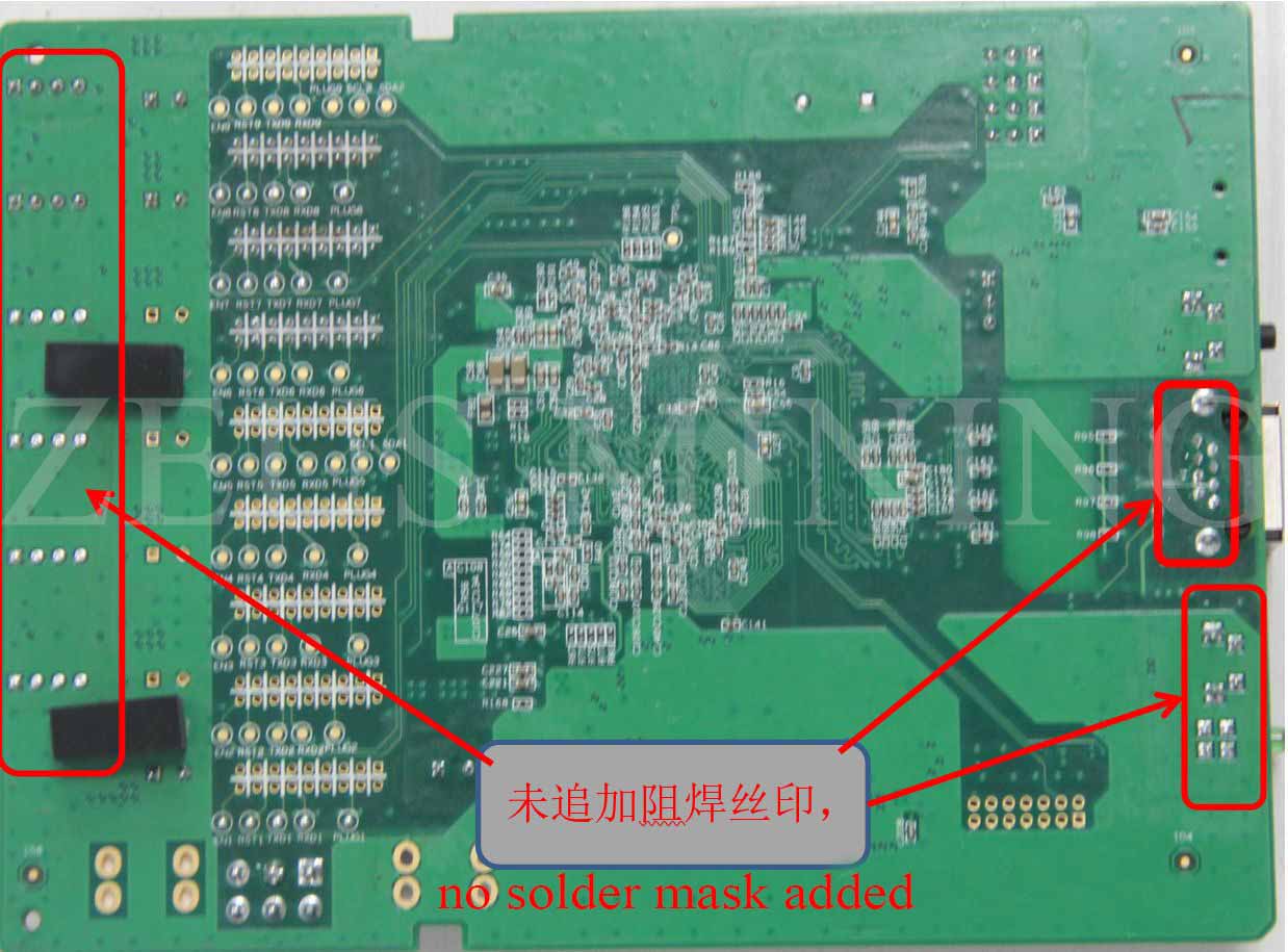
3. The DIP flow direction indication is not added to the PCB LAYOUT, and the ETH socket and fan sockets FAN1~FAN6 are not added with solder resist silkscreen, so it is easy to connect tin during wave soldering.
5. The cost of PCBA is high. TI DC-DC products can choose MPS or Taiwan GMT series products for cost down in terms of chip selection.
III. Analysis of mining revenue
Antminer S9 can mine Bitcoin and 41 other coins. However, according to the miner income network calculation, miners' current daily electricity cost is $3.95, the daily output is $3.06, and the daily net income is -$0.89. Therefore, according to the current market, S9 is no longer profitable. For more profitability of Antminer S9, please check the article How profitable is Antminer S9?(内链) for more details!








Comments
Post a Comment
Tell us your opinion