ASIC Miner ICERIVER KAS KS0 Profitability In the realm of cryptocurrency mining, the Iceriver KAS KS0 miner has garnered widespread attention. Tailored specifically for the Kaspa network's KHeavyHash algorithm, it boasts high hashing power and low power consumption, making it an ideal choice for many miners. In this article, we will comprehensively assess IceRiver KS0 profitability while considering the Kaspa market conditions and the attributes of KS0 miner. Kaspa Market Dynamics Kaspa is a vibrant cryptocurrency network aimed at delivering high performance and scalability for everyday transactions. At the time of writing this article, the Kaspa coin trades at approximately $0.04959. But it's essential to note that cryptocurrency markets are highly susceptible to price volatility. Hence, investors must remain vigilant about market dynamics. Additionally, the Kaspa network's mining difficulty and reward mechanisms play a role in mining returns. Attributes of the IceRiver KS...
How many kinds of chips are on the Innosilicon T2TH+ hash board?
When you see the Innosilicon T2TH+ hash board for the first time, you will find that it is very different from other hash boards. It uses six independent heat sinks on the front and a whole upgraded heat sink on the back. In addition to the heat sink, there are many chips with different functions on the front. So what types of chips are there? Through this article, let's find out together!
LC2001A ASIC chip
Below this independent heat sink is the Innosilica T2TH+ ASIC chip. The entire hash board has a total of 140 LC2001B ASIC chips.
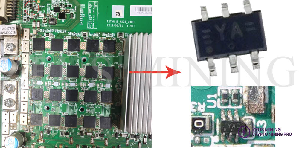
Chip name: 74LVC2G34GW
Chip location: U1
Chip silkscreen: YA
The 74LVC2G34GW is a 6-pin double buffer logic chip in a SOT-363 package. The wide supply voltage range is between 1.65 V and 5.5 V, and the operating temperature is between -40°C and +125°C. Therefore, the device is fully suitable for partial-power-down applications using IOFF. The IOFF circuit disables the output, preventing damaging backflow currents from passing through.
Chip name: MP3426
Chip location: U3
Chip silkscreen: MPKG3426971
The MP3426 is a current-mode boost converter with a programmable switching frequency and UVLO evaluation board in a QFN-14 (3mm*4mm) package with an exposed pad, with a 6A, 90mΩ internal switch that provides a fast response High-Efficiency Regulator. The MP3426 has a programmable frequency of up to 2MHz for easy filtering and noise reduction. External compensation pins allow users to set loop dynamics and use small, low ESR ceramic output capacitors. The device operates from input voltages as low as 3.2V and can generate outputs as high as 35V. In addition, the MP3426 includes an Undervoltage lockout, current limit and thermal overload protection.
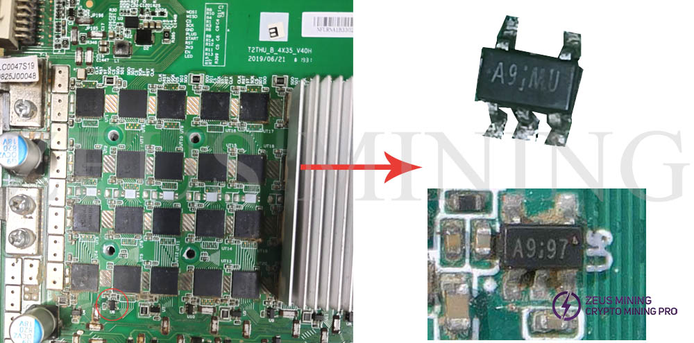
Chip name: SI9183DT-AD-T1
Chip location: U6
Chip silkscreen: A9i97
SI9183DT-AD-T1 is an LDO linear regulator with silkscreen A9***, 150mA adjustable in a SOT23-5 package, and 1.5V-5V output power management IC. It is compatible with KF1921 of Whatsminer M21S hash board The chip is LDO power supply relationship, LDO power supply to the chip signal transmission is normal, each layer has an LDO chip power supply, pin 5 output, the voltage is 1.8V, the voltage is divided by 0.9V and then sent to the chip. Its operating temperature is between -40°C to +85°C, and the operating input voltage is between 2V and 6V.


Comments
Post a Comment
Tell us your opinion